Innovative and Sustainable Semiconductor Fabrication Processes are the Common Goal
The center for micro- and nanotechnologies (ZfM) at Chemnitz University of Technology takes the lead in the European collaborative project HaloFreeEtch, funded with almost four million Euro by the EU.
-

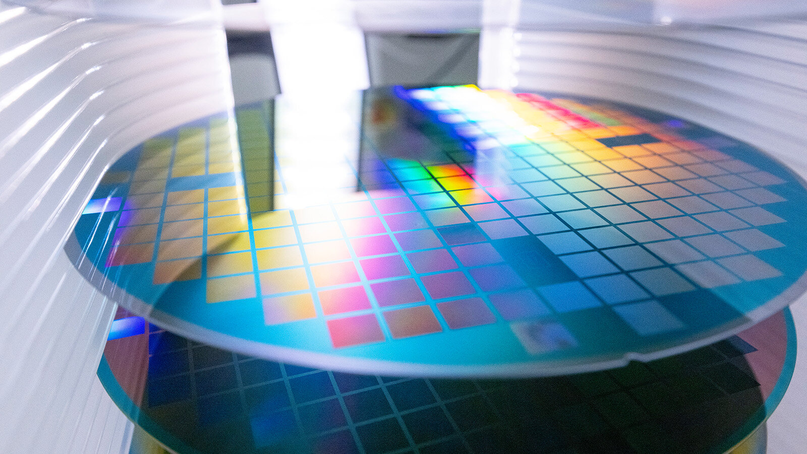
Silicon Wafer after etching for dry structuring in the clean room of the center for micro- and nanotechnologies at Chemnitz university of technology. Photo: Jacob Müller
The center for micro- and nanotechnologies (ZfM) at Chemnitz University of Technology coordinates the recently started European project HaloFreeEtch to explore novel and sustainable processes for semiconductor manufacturing. The project aims to develop sustainable and halogen-free etching processes for the semiconductor industry by reducing the use of halogene-containing chemicals and energy consumption.
Established semiconductor etching processes rely on halogene-containing materials which pose significant environmental and health risks. Thus, scientists from the ZfM will explore novel approaches to etch silicon or glass by using hydrogen and innovative catalysts. Using such environmentally friendly alternatives will reduce the ecological footprint of the sector significantly.
At the ZfM, quantum chemical simulation methods will be used to screen promising materials on the computer in front of lab scale research to explore the process performance in the clean room environment on state-of-the-art equipment. Together with the partners, novel methodologies for sustainability-driven process development will be established. By combining process- and sustainability models, the use of critical materials as well as the consumption of energy will be tracked and optimized.
“For us it is very important, that the new semiconductor processes are not only environmentally friendly, but also meet the performance requirements of the modern semiconductor industry, leading the industry into a more sustainable future.” says Dr. Jörg Schuster from Chemnitz University of Technology, who is coordinating the European project.
Funded with about four million Euro from the EU, HaloFreeEtch will run for four years. The project consortium involves several leading European research and industry partners, among them the Fraunhofer Institute for Electronic Nano Systems (ENAS) in Chemnitz. The results are expected not only to revolutionize semiconductor manufacturing but also enable applications in areas such as microsensors and photonics.
More information on the project website: https://halofreeetch.eu/
Contact: Dr. Jörg Schuster Technische Universität Chemnitz, Email joerg.schuster@zfm.tu-chemnitz.de
(Author and Translation: Dr. Jörg Schuster)
Mario Steinebach
30.10.2024


